News Center
Your Location : Home >> News Center
-
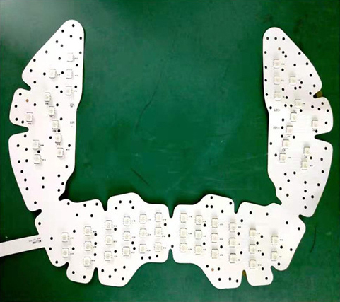 1. Correct components:SMT patch processing requires that the type, model, nominal value and polarity of each assembly number component must comply with the product assembly drawing and BOM requirements, and must not be pasted in the wrong position.2. Accurate position:During SMT patch processing, the ends or pins of the components should be aligned and centered with the pad pattern as much as possible, and it is also necessary to ensure that the component solder end contacts the solder paste pattern.The self-positioning effect of the chip components at both ends is relatively large. When mounting, more than 3/4 of the width direction of the component overlaps the pad, and the two ends in the length direction overlap the corresponding pad and contact the solder paste pattern. It can be self···
 -
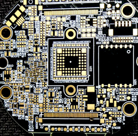 Problems with SMT patch processing production materials will lead to failure to mount normally and low patch processing yield. In order to help everyone avoid these problems, based on our company's many years of patch processing experience, we summarize them as follows.Common problems with SMT patch processing production materials1. The absence of marking points and process edges on the PCB board will cause the components on the PCB rail side of the SMT patch machine to fail to stick, and the lack of marking points will lead to low correction accuracy at smaller positions on the PCB board.2. The SMT components do not correspond to the SMT pads on the PCB board. For example, the SMD pads are too wide or too narrow to match the SMD components.3. There are past holes on the SMT pads.4. Co···
 -
 Traditionally, the electrical connection between IC chips and the outside is achieved by bonding the I/O on the chip to the package carrier through the package pins using metal wires. With the reduction of IC chip feature size and the expansion of integration scale, the spacing of I/O is constantly decreasing and the number is constantly increasing. When the I/O spacing is reduced to below 70 um, the wire bonding technology is no longer applicable, and new technical approaches must be sought. Wafer-level packaging technology uses thin film redistribution technology to allow I/O to be distributed on the entire surface of the IC chip instead of being limited to the narrow peripheral area of the IC chip, thereby solving the electrical connection problem of high-density, fine-pitch I/O chips.A···
