News Center
-
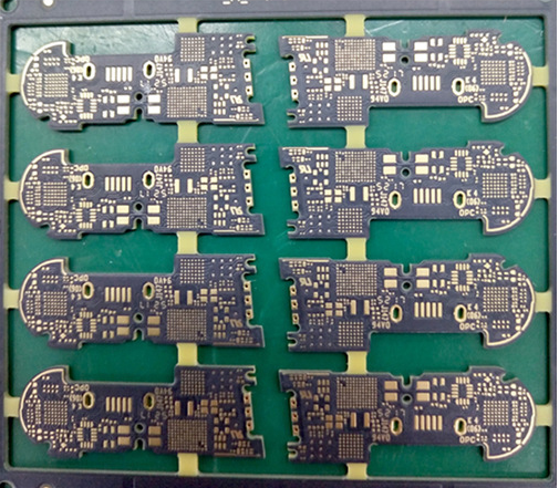 Traditionally, the electrical connection between IC chips and the outside is achieved by bonding the I/O on the chip to the package carrier through the package pins using metal wires. With the reduction of IC chip feature size and the expansion of integration scale, the spacing of I/O is constantly decreasing and the number is constantly increasing. When the I/O spacing is reduced to below 70 um, the wire bonding technology is no longer applicable, and new technical approaches must be sought. Wafer-level packaging technology uses thin film redistribution technology to allow I/O to be distributed on the entire surface of the IC chip instead of being limited to the narrow peripheral area of the IC chip, thereby solving the electrical connection problem of high-density, fine-pitch I/O chips.A···
